| CPC H03L 7/0816 (2013.01) [G11C 11/4076 (2013.01)] | 19 Claims |
|
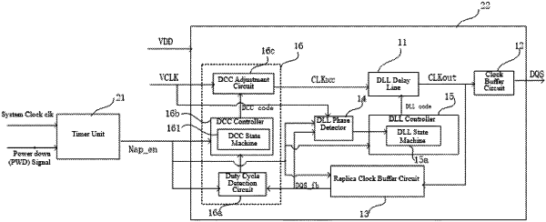
1. Delay locked loop (DLL) circuitry system, comprising:
a DLL circuit configured to receive an external clock signal and generate an internal clock signal delayed relative to the external clock signal and lock the internal clock signal in phase with the external clock signal; and
a timer unit coupled to an enable terminal of the DLL circuit and configured to be enabled in response to a signal instructing entry into a low power consumption mode from outside of the DLL circuitry system and generate, based on the signal instructing entry into the low power consumption mode and a predefined timer condition, a DLL enable signal which enables the DLL circuit to allow the DLL circuit to relock the internal clock signal in phase with the external clock signal.
|