| CPC H03K 5/135 (2013.01) [H03K 5/2418 (2013.01); H03K 5/2427 (2013.01); H03K 2005/00176 (2013.01)] | 16 Claims |
|
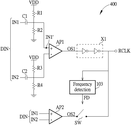
1. An input clock buffer, comprising:
a first capacitor;
a second capacitor;
a first amplifier, configured to generate a first output signal, comprising a first input terminal coupled to the first capacitor and comprising a second input terminal coupled to the second capacitor, wherein the first capacitor and the second capacitor receives a differential input signal and form a first pair of signal paths for the differential input signal;
a second amplifier, configured to generate a second output signal, comprising a first input terminal and a second input terminal, wherein the first input terminal of the second amplifier and the second input terminal of the second amplifier form a second pair of signal paths for the differential input signal;
a frequency detection circuit, configured to generate a frequency detection signal according to a frequency of the differential input signal; and
a switch, located between an output of the first amplifier and an output of the second amplifier, configured to turn on and turn off according to the frequency detection signal.
|