| CPC H03K 5/086 (2013.01) [H03K 3/354 (2013.01)] | 20 Claims |
|
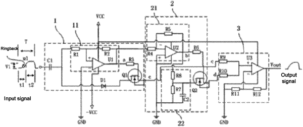
1. A signal correction circuit, comprising:
a first signal processing component, configured to receive an input signal, positive power supply voltages and negative power supply voltages, generate a first control voltage according to the input signal, the positive power supply voltages and negative power supply voltages, control the input signal according to the first control voltage, and output a first voltage, the first voltage is zero within a first time period, and the waveform of the first voltage in a second time period is the same as the waveform of the input signal;
a second signal processing component, electrically connected to the first signal processing component, and configured to generate a second control voltage according to the first control voltage, perform energy storage charging according to the second control voltage, control an energy storage charging voltage according to the second control voltage, and output a second voltage, the corresponding waveform of the second voltage in the first time period comprises a smooth monotonic rising curve and a straight line connected to the smooth monotonic rising curve, and the second voltage is zero in the second time period; and
an output component, electrically connected to each of the first signal processing component and the second signal processing component respectively, and configured to perform superposition processing on the first voltage and the second voltage to obtain an output signal, the waveform of the output signal in the first time period is the same as the waveform of the second voltage in the first time period, and the waveform of the output signal in the second time period is the same as the waveform of the first voltage in the second time period.
|