| CPC H03K 3/012 (2013.01) [H01L 29/0607 (2013.01); H01L 29/1045 (2013.01); H01L 29/7826 (2013.01); H03K 3/356182 (2013.01)] | 20 Claims |
|
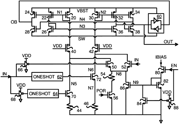
1. A level shifter comprising:
a switch-control input;
a first oneshot for generating a first pulse in response to a falling-edge transition of the switch-control input;
a second oneshot for generating a second pulse in response to a rising-edge transition of the switch-control input;
a first transient differential transistor, having a gate receiving the first pulse and a drain connected to a first node;
a first voltage-tolerant transistor having a gate driven by a gate bias voltage and a source connected to the first node and a drain connected to a third node;
a first sensing transistor having a gate and a drain connected to the third node and a source connected to a boosted node;
a second transient differential transistor, having a gate receiving the second pulse and a drain connected to a second node;
a second voltage-tolerant transistor having a gate driven by the gate bias voltage and a source connected to the second node and a drain connected to a fourth node;
a second sensing transistor having a gate and a drain connected to the fourth node and a source connected to the boosted node;
an upper buffer for buffering the third node to generate an inverted output, and for buffering the fourth node to generate an output; and
a bistable latch receiving the output and receiving the inverted output, the bistable latch for latching the output and the inverted output;
wherein the upper buffer and the bistable latch are each powered by the boosted node and has a floating ground node;
wherein the first transient differential transistor and the second transient differential transistor are each an n-channel transistor having a standard-n source-drain breakdown voltage;
wherein the first sensing transistor and the second sensing transistor are each a p-channel transistor having a standard-p source-drain breakdown voltage;
wherein the first voltage-tolerant transistor and the second voltage-tolerant transistor are each an enhanced n-channel transistor fabricated to have an enhanced source-drain breakdown voltage that is greater than the standard-n source-drain breakdown voltage,
whereby voltage-tolerant enhanced transistors are placed between the upper buffer and the first and second transient differential transistors.
|