| CPC H03K 19/17724 (2013.01) [H03K 19/1737 (2013.01); H03K 19/1774 (2013.01); H03K 19/17744 (2013.01); H03K 19/20 (2013.01)] | 16 Claims |
|
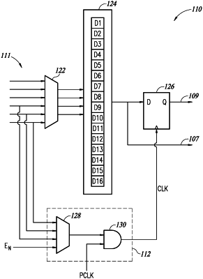
1. A method, comprising:
receiving a plurality of input signals at a first multiplexer of first logic cell of a programmable logic array;
providing a subset of the plurality of input signals to a second multiplexer;
receiving a global clock signal at a first input of an AND gate;
receiving a selected input signal of the plurality of input signals at a second input of the AND gate;
outputting the selected input signal from the multiplexer to a second input of the AND gate, and
supplying a clock signal from the AND gate to a clock input terminal of a flip-flop of the first logic cell.
|