| CPC H03K 19/018521 (2013.01) [H03K 3/0375 (2013.01); H03K 19/00315 (2013.01)] | 10 Claims |
|
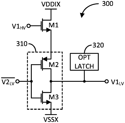
1. An apparatus, comprising:
a first field effect transistor (FET) comprising an n-channel metal oxide semiconductor (NMOS) FET, including a first gate configured to receive a first input signal that varies in accordance with a first voltage domain; and
a first inverter including a first input configured to receive a second input signal that varies in accordance with a second voltage domain, and a first output configured to generate a first output signal that varies in accordance with the second voltage domain, wherein the first output signal is based on the first and second input signals, and wherein the first FET and the first inverter are coupled in series between first and second voltage rails,
wherein the first and second voltage rails are configured to receive first and second supply voltages in accordance with the second voltage domain, respectively, and further
wherein the NMOS FET and the first inverter are coupled in series in that order between the first voltage rail and the second voltage rail.
|