| CPC H03K 17/693 (2013.01) [H03K 17/04123 (2013.01); H03K 17/162 (2013.01); H03K 2217/0081 (2013.01)] | 16 Claims |
|
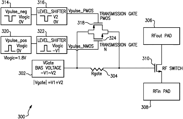
1. A switching circuit comprising:
a radio frequency (RF) switch including a gate;
a gate resistor coupled at a first side of the gate resistor to the gate the RF switch at a first node;
a voltage source coupled to a second side of the gate resistor at a second node;
a transmission gate including a first semiconductor and a second semiconductor, the transmission gate being coupled to the first side of the gate resistor and the gate of the RF switch at the first node and further being coupled to the voltage source and the second side of the gate resistor at the second node;
a first level shifter coupled to the first semiconductor and configured to supply voltage pulses to the first semiconductor; and
a second level shifter coupled to the second semiconductor and configured to supply voltage pulses to the second semiconductor.
|