| CPC H03K 17/223 (2013.01) [G05F 3/262 (2013.01)] | 6 Claims |
|
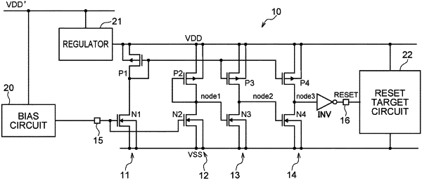
1. A semiconductor device that outputs a reset signal for controlling a reset operation of a reset target circuit connected to a first power supply and a second power supply having a voltage lower than a voltage of the first power supply, the semiconductor device comprising:
a power supply voltage monitoring circuit connected to the first power supply and the second power supply, the power supply voltage monitoring circuit monitors the voltage of the first power supply; and
a current mirror circuit to which a predetermined voltage is supplied to cause a first current to flow, wherein the current mirror circuit transmits a second current based on the first current to another transistor,
wherein the power supply voltage monitoring circuit includes a first transistor having a first conductive type and a second transistor having a second conductive type different from the first conductive type,
wherein the reset signal is switched when the voltage of the first power supply is equal to or greater than a sum of a threshold voltage of the first transistor, and a threshold voltage of the second transistor,
wherein the power supply voltage monitoring circuit includes a first power supply voltage monitoring circuit including the first transistor and a second power supply voltage monitoring circuit including the second transistor,
wherein the first transistor is diode-connected,
wherein a control terminal of the second transistor is connected to a control terminal of the first transistor,
wherein the first power supply voltage monitoring circuit includes a third transistor connected to the control terminal of the first transistor, the first power supply voltage monitoring circuit receives the second current from the current mirror circuit and causes a third current to flow to the first transistor, and
wherein the second power supply voltage monitoring circuit includes a fourth transistor connected to a first terminal of the second transistor, the second power supply voltage monitoring circuit receives the second current from the current mirror circuit and causes a fourth current to flow to the second transistor.
|