| CPC H03H 9/145 (2013.01) [H03H 9/02007 (2013.01); H03H 9/02535 (2013.01); H03H 9/25 (2013.01)] | 9 Claims |
|
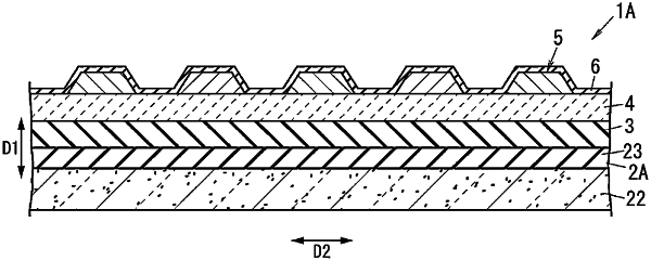
1. An acoustic wave device comprising:
a piezoelectric layer;
an interdigital transducer (IDT) electrode located on the piezoelectric layer;
a high-acoustic-velocity member positioned on an opposite side of the piezoelectric layer from the IDT electrode such that an acoustic velocity of a bulk wave propagating through the high-acoustic-velocity member is higher than an acoustic velocity of an acoustic wave propagating through the piezoelectric layer;
a low-acoustic-velocity film provided between the high-acoustic-velocity member and the piezoelectric layer such that an acoustic velocity of a bulk wave propagating through the low-acoustic-velocity film is lower than the acoustic velocity of the bulk wave propagating through the piezoelectric layer; and
a dielectric film located on the piezoelectric layer so as to cover the IDT electrode; wherein
a Young's modulus of the dielectric film is larger than a Young's modulus of the low-acoustic-velocity film; and
a material of the dielectric film is silicon oxide.
|