| CPC H03H 3/02 (2013.01) [H03H 9/02031 (2013.01); H03H 9/174 (2013.01); H03H 9/176 (2013.01); H03H 2003/023 (2013.01); Y10T 29/42 (2015.01)] | 20 Claims |
|
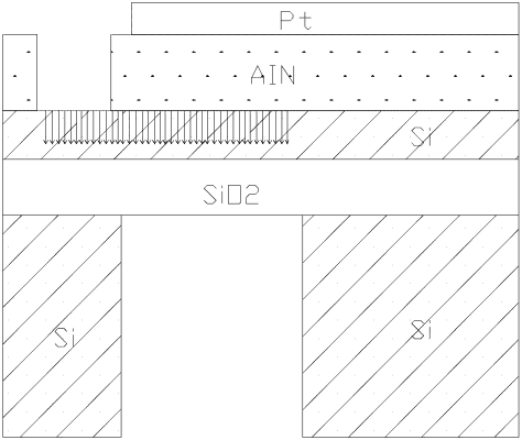
1. A fabricating method of a film bulk acoustic resonator, comprising:
fabricating a lower electrode on a first surface of an SOI substrate by treating a top silicon of the SOI substrate using an ion implantation method to at least make a selected region of the top silicon into a highly doped conductive silicon layer and patterning the highly doped conductive silicon layer to obtain the lower electrode, such that the patterned highly doped conductive silicon layer formed in the selected region of the top silicon is used as the lower electrode, wherein the SOI substrate comprises the top silicon, a back substrate, and an oxidation layer arranged between the top silicon and the back substrate;
forming a piezoelectric layer on the first surface of the SOI substrate and the lower electrode;
forming top electrodes on the piezoelectric layer; and
processing an air cavity on a second surface of the SOI substrate, wherein the second surface and the first surface are oppositely arranged, and wherein the air cavity is below the oxidation layer and the air cavity is formed in the back substrate.
|