| CPC H03G 3/3042 (2013.01) [H01P 5/18 (2013.01); H03D 1/10 (2013.01); H03F 3/24 (2013.01); H04B 1/04 (2013.01)] | 19 Claims |
|
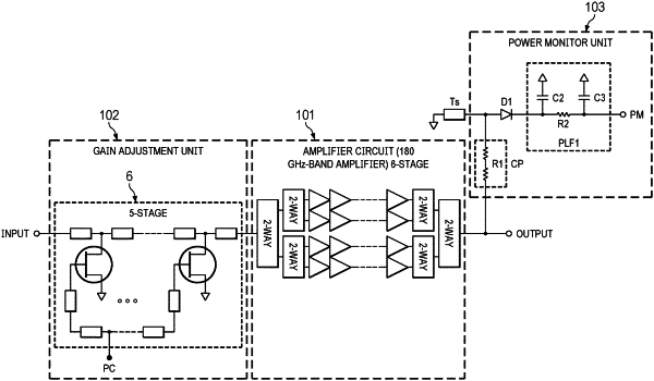
1. A variable gain amplifier, comprising:
a gain adjuster comprising a switch having a control terminal in an input of an amplifier circuit; and
a power monitor branched in an output of the amplifier circuit, wherein the power monitor comprises:
a coupler, a first end of the coupler being connected to an output line of the amplifier circuit;
a diode, an anode of the diode being connected to a second end of the coupler; and
a monitor terminal connected to a cathode of the diode via a low-pass filter, the anode of the diode being set to ground potential.
|