| CPC H03F 3/245 (2013.01) [H03F 1/0288 (2013.01); H03F 1/26 (2013.01); H03F 2200/451 (2013.01); H03F 2203/21127 (2013.01)] | 20 Claims |

|
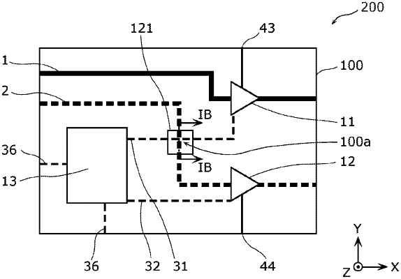
1. A radio-frequency power amplifier device that is a radio-frequency power amplifier device of a hybrid type in which a carrier amplifier semiconductor device and a peak amplifier semiconductor device are disposed on a principal surface of a multilayer submount substrate, the multilayer submount substrate including a plurality of resin layers and a plurality of wiring layers, the radio-frequency power amplifier device comprising:
a bias power supply semiconductor device that outputs a carrier-amplifier bias power supply voltage to the carrier amplifier semiconductor device, and outputs a peak-amplifier bias power supply voltage to the peak amplifier semiconductor device;
radio-frequency signal wiring that is wired in a first wiring layer provided on the principal surface, and transmits a radio-frequency signal to the carrier amplifier semiconductor device or the peak amplifier semiconductor device; and
bias power supply wiring that is wired in a third wiring layer of the multilayer submount substrate, and supplies the carrier-amplifier bias power supply voltage to the carrier amplifier semiconductor device or supplies the peak-amplifier bias power supply voltage to the peak amplifier semiconductor device,
wherein the multilayer submount substrate includes an intersection portion in which, in a plan view of the multilayer submount substrate, the radio-frequency signal wiring and the bias power supply wiring intersect,
the intersection portion includes:
a shield pattern that is a portion of a second wiring layer disposed between the first wiring layer and the third wiring layer, and is set to a ground electric potential; and
a ground connection via that is disposed on each of both sides of a width of the bias power supply wiring, within a distance from the bias power supply wiring that is three times as large as the width of the bias power supply wiring in an extension direction of the bias power supply wiring, and is set to a ground electric potential.
|