| CPC H03F 3/005 (2013.01) [H03F 3/45179 (2013.01); H03F 2203/45244 (2013.01)] | 19 Claims |
|
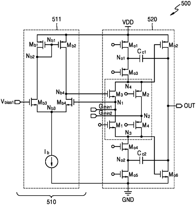
1. An amplifier comprising:
an input circuit configured to convert an input signal into a current;
an output circuit comprising at least one switching element and configured to provide an output signal; and
a biasing circuit connected to the at least one switching element of the output circuit to form a feedback loop configured to adjust a voltage change of an output end of the input circuit,
wherein the biasing circuit comprises a first input node connected to a first operating voltage of the amplifier and a second input node connected to a source node of the at least one switching element,
wherein the output end of the input circuit is connected to the source node of the at least one switching element, and
wherein the output circuit further comprises a capacitor configured to increase a bandwidth of the output signal.
|