| CPC H03F 1/30 (2013.01) [H03F 1/32 (2013.01); H03F 3/04 (2013.01); H03F 2200/447 (2013.01)] | 20 Claims |
|
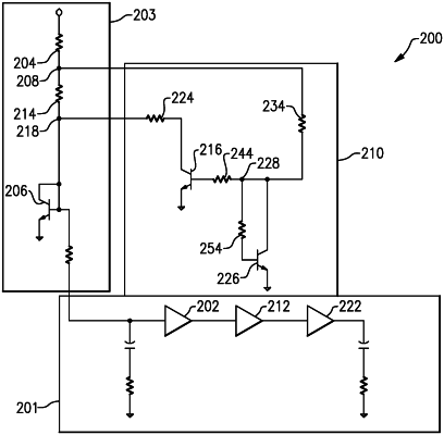
1. A circuit comprising:
an amplifier network including a first amplifier;
a first transistor having a first base, a first emitter, and a first collector, the first transistor being thermally isolated from the first amplifier;
a second transistor having a second base, a second emitter, and a second collector, the second transistor being thermally linked to the first amplifier;
a bias network configured to bias the amplifier network with a reference current; and
coupling circuitry configured to couple the first base to the second base, the first collector to the bias network, and the second collector to the bias network.
|