| CPC H03B 5/32 (2013.01) [H10N 30/06 (2023.02); H10N 30/082 (2023.02); H03B 2200/0022 (2013.01)] | 7 Claims |

|
1. A method for making a crystal oscillator, comprising the steps of:
a) forming a first electrode portion on a surface of a piezoelectric substrate, so as to obtain a first semi-finished product;
b) attaching the first semi-finished product on a temporary substrate with the first electrode portion facing the temporary substrate;
c) thinning the piezoelectric substrate of the first semi-finished product, so as to obtain a thinned piezoelectric substrate having a first thickness and having a first surface on which the first electrode portion is formed;
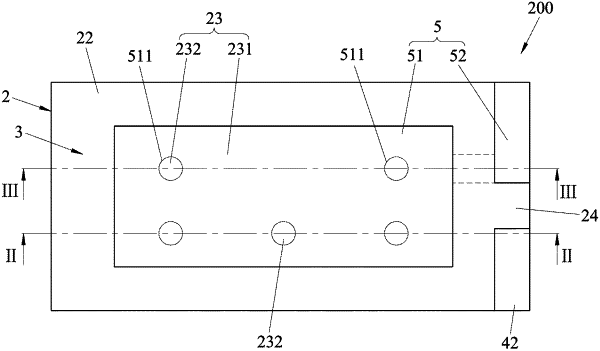
d) forming a second electrode on a second surface of the thinned piezoelectric substrate opposite to the temporary substrate, the second electrode including a second electrode portion having at least one opening, and a second extending electrode portion extending outwardly from the second electrode portion and disposed on a peripheral region of the thinned piezoelectric substrate, a projection of the second electrode portion on the second surface of the thinned piezoelectric substrate partially overlapping a projection of the first electrode portion on the second surface of the thinned piezoelectric substrate;
e) forming a first extending electrode portion that extends from the first electrode portion along a side surface of the thinned piezoelectric substrate to the second surface of the thinned piezoelectric substrate;
f) forming a hollow frame on the second surface of the thinned piezoelectric substrate, the hollow frame surrounding the second electrode portion, and disposed on the second extending electrode portion; and
g) etching a portion of the thinned piezoelectric substrate in positional correspondence with the at least one opening using the second electrode as a mask.
|