| CPC H02N 13/00 (2013.01) [A61F 2/02 (2013.01); A61F 2002/0086 (2013.01); A61F 2/482 (2021.08)] | 18 Claims |
|
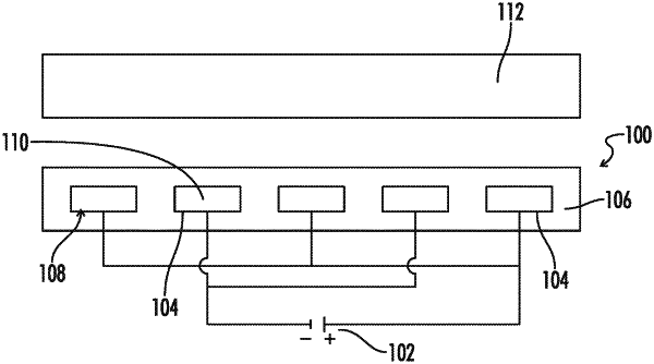
1. An electro-microstructured device comprising:
a substrate having a hierarchical microstructure disposed thereon, the substrate having a thickness;
the hierarchical microstructure having a first microfeature, the first microfeature having a surface wherein a plurality of second microfeatures are disposed about the surface of the first microfeature; and
a first electrode and a second electrode, the first electrode and second electrode at least partially embedded within the thickness of the substrate and connected to a charge source, wherein the first electrode is configured to provide a positive charge of about +0.5V and the second electrode is configured to provide a negative charge of about −0.5V when powered by the charge source, and wherein charging the first electrode and second electrode generates an electroadhesive state via Wenzel-Cassie wetting domains.
|