| CPC H02M 3/07 (2013.01) [H03F 3/191 (2013.01); H03F 3/245 (2013.01); H03F 3/72 (2013.01); H02M 1/0003 (2021.05); H03F 2200/111 (2013.01); H03F 2203/7209 (2013.01)] | 20 Claims |
|
1. A wireless device comprising:
a transceiver configured to process a radio-frequency signal;
an antenna in communication with the transceiver, the antenna configured to transmit an amplified radio-frequency signal; and
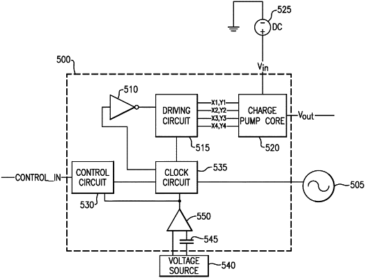
a radio-frequency module in communication with the transceiver and the antenna, the radio-frequency module including a voltage supply system, the voltage supply system including a charge pump module, the charge pump module including a control circuit configured to generate a first control signal and a second control signal based on an output of a comparator, a clock circuit configured to generate a first clock signal in response to receiving the first control signal and a second clock signal in response to receiving the second control signal, the first clock signal having a different frequency from the second clock signal, the clock circuit coupled to the output of the comparator, the control circuit coupled to the output of the comparator, the comparator including a first input provided with a voltage representative of a single input voltage of the charge pump module that is used to generate an output voltage of the charge pump module and a second input provided with a voltage of the single input voltage through a timing capacitance such that the clock circuit is provided with the first control signal when the voltage of the first input is less than the voltage of the second input and the clock circuit is provided with the second control signal when the voltage of the first input is equal to or greater than the voltage of the second input, a driving circuit configured to generate a first set of clock signals based on the first clock signal and a second set of clock signals based on the second clock signal, the driving circuit coupled to the clock circuit, and a charge pump core including a set of capacitances, the charge pump core configured to charge the set of capacitances based on the first set of clock signals and the second set of clock signals.
|