| CPC H02M 3/07 (2013.01) [H02M 1/08 (2013.01); H03K 17/687 (2013.01)] | 13 Claims |
|
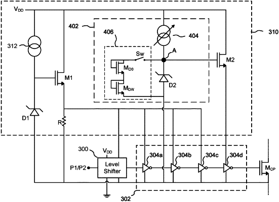
1. A gate control circuit for controlling current flow through a power FET having a gate, the gate control circuit including:
(a) a voltage control circuit including a first selectable configuration electrically disconnected from a node, and a second selectable configuration electrically coupled to the node, wherein the node has a first voltage in the first selectable configuration and a lower second voltage in the second selectable configuration; and
(b) a voltage supply device having a gate coupled to the node and a conduction channel configured to be coupled to the gate of the power FET and to provide an output voltage to the gate of the power FET in response to the voltage at the node, wherein an ON resistance, RON, of the power FET in a first ON state is lowered when the voltage control circuit is in the first selectable configuration during normal operation of the power FET and current flow through the power FET in a second ON state is restricted when the voltage control circuit is in the second selectable configuration.
|