| CPC H02H 9/046 (2013.01) [H01L 27/0285 (2013.01)] | 14 Claims |
|
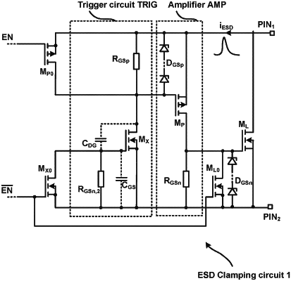
1. A circuit comprising:
a first transistor including a control terminal and a load current path connected between a first contact and a second contact;
a first amplifier circuit including an amplifier input and an amplifier output, the amplifier output connected to the control terminal of the first transistor;
a trigger circuit connected between the first contact and the second contact, the trigger circuit comprising:
a first resistor connected between the amplifier input and the first contact;
a second transistor including a control terminal, a first node, and a second node,
the second transistor comprising an intrinsic capacitance coupling the first node of the second transistor to the control terminal of the second transistor, wherein the second node of the second transistor is coupled to the second contact; and
a second resistor connected between the control node of the second transistor and the second contact,
wherein the trigger circuit is configured to operate the second transistor in a conducting state in response to a voltage produced across the second resistor as a result of a discharge current from the first contact that flows from the first resistor to the control terminal of the second transistor via the intrinsic capacitance of the second transistor and from the control node to the second contact via the second resistor,
wherein operating the second transistor in the conducting state generates a voltage swing at the amplifier input; and
an enable circuit comprising a first enable transistor including a load current path connected between the first contact and the amplifier input, wherein the first enable transistor is configured to deactivate the amplifier circuit based on a logic signal.
|