| CPC H01S 5/4031 (2013.01) [B23K 26/122 (2013.01); H01S 5/0237 (2021.01); H01S 5/02469 (2013.01); H01S 5/02492 (2013.01); H01S 5/04254 (2019.08); H01S 5/22 (2013.01); H01S 5/32341 (2013.01); H01S 5/02345 (2021.01); H01S 5/04256 (2019.08)] | 12 Claims |
|
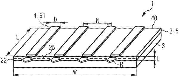
1. A semiconductor laser comprising:
a semiconductor layer sequence on a basis of a material system AlInGaN with at least one active zone, and
at least one heat sink to which the semiconductor layer sequence is thermally connected and to which the semiconductor layer sequence has a thermal resistance,
wherein the semiconductor layer sequence is divided into a plurality of emitter strips and each emitter strip has a width between 15 μm and 150 μm inclusive in a direction perpendicular to a beam direction, the emitter strips are arranged with a filling factor (FF) of between 0.07 and 0.18 inclusive and the filling factor (FF) is a quotient of a width b of the emitter strips and a periodicity N of the emitter strips,
the semiconductor layer sequence is attached by a solder to the heat sink and the solder extends over an entire surface and uninterruptedly between the semiconductor layer sequence and the at least one heat sink, and
the semiconductor layer sequence is located on a growth substrate thereof and the growth substrate is located on a side of the semiconductor layer sequence facing away from the heat sink,
wherein the following applies to the filling factor (FF) as a function of thermal resistance Rth:
FF=(0.18W2/K2Rth2−0.40W/K Rth+0.30)±0.02,
wherein each of the emitter strips are each configured as strip waveguides, wherein the at least one active zone is removed between adjacent emitter strips,
wherein the at least one heat sink is attached by a soft solder to the semiconductor layer sequence, wherein the soft solder comprises indium and the at least one heat sink is a microchannel cooler.
|