| CPC H01S 5/1014 (2013.01) [H01S 5/026 (2013.01); H01S 5/0264 (2013.01); H01S 5/12 (2013.01); H01S 5/16 (2013.01)] | 19 Claims |
|
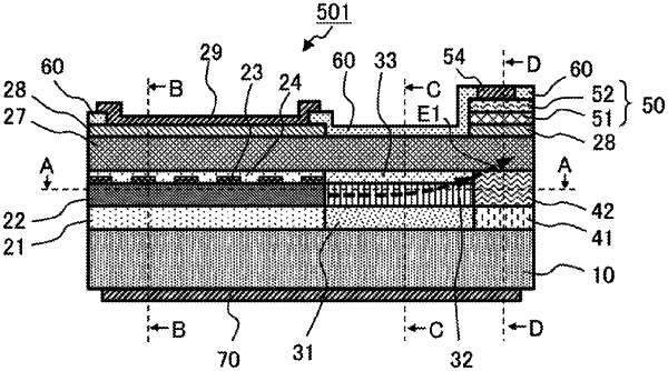
1. An optical semiconductor integrated element, comprising:
a laser diode section provided on a surface of a substrate;
a spot-size converter section provided on a surface of the substrate, said spot-size converter section being composed of: a core layer which causes laser light emitted from the laser diode section to propagate therein and whose both sides are tapered down in a propagation direction of the laser light to form a tapered shape; a front-surface side cladding layer which covers a front surface side of the core layer; a back-surface side cladding layer which covers a back surface side of the core layer; first cladding layers provided on the both sides of the core layer; and a second cladding layer provided on respective surfaces of the front-surface side cladding layer and the first cladding layers;
a window region provided on a surface of the substrate that is placed on a front-end side of the core layer of the spot-size converter section; and
a monitor section provided on a surface of the window region;
wherein a refractive index of the first cladding layers is lower than a refractive index of the second cladding layer.
|