| CPC H01S 5/0421 (2013.01) [H01S 5/042 (2013.01); H01S 5/343 (2013.01)] | 22 Claims |
|
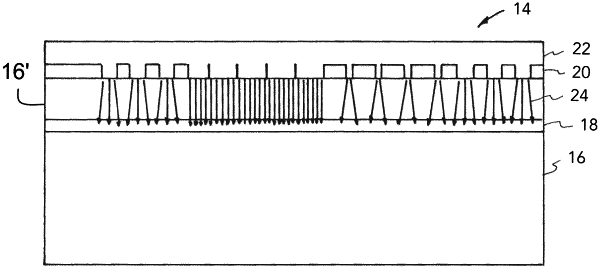
1. An engineered current-density profile diode laser, comprising:
a first portion of semiconductor material;
a quantum well active region on said first portion of semiconductor material;
a second portion of said semiconductor material on said quantum well active region;
a metal contact on said second portion of said semiconductor material; and
a plurality of current vias located between said quantum well active region and said metal contact,
wherein said current vias provide, in use, a desired current density per longitudinal direction of said diode laser;
said current density increasing from a zero value to a first value at a first position along said longitudinal direction,
said current density increasing from said first value to a second value at a second position along said longitudinal direction,
said current density decreasing from said second value to a third value, lower than the first value, at a third position along said longitudinal direction, and
said current density increasing from said third value to said first value at a fourth position along said longitudinal direction.
|