| CPC H01S 5/0235 (2021.01) [H01S 5/023 (2021.01); H01S 5/02345 (2021.01); H01S 5/028 (2013.01); H01L 2224/48227 (2013.01)] | 20 Claims |
|
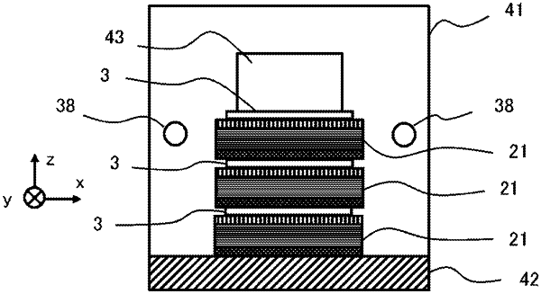
1. A semiconductor laser device manufacturing method of manufacturing a semiconductor laser device in which a protective film is formed on cleaved end faces of a semiconductor laser bar which is a bar-shaped semiconductor laser, the method comprising:
a material preparation step of forming a metal layer on a front side surface of a bar-shaped submount bar body which is to face the semiconductor laser bar, to prepare a bar-shaped submount bar on which the semiconductor laser bar is to be mounted, wherein the semiconductor laser bar has a front side electrode formed on one surface different from the cleaved end faces and has a back side electrode formed on a surface opposite to the one surface;
a jig installation step of installing the submount bar and the semiconductor laser bar that are provided in plural number alternately stacked on an installation jig such that the metal layer of the submount bar and the back side electrode of the semiconductor laser bar face each other;
a bonding step of bonding the metal layer and the back side electrode by increasing a temperature of the installation jig in which the submount bar and the semiconductor laser bar that are provided in plural number are installed; and
a protective film forming step of forming the protective film on the cleaved end faces of the semiconductor laser bar in a protective film forming apparatus using the installation jig in which the submount bar and the semiconductor laser bar that are provided in plural number are installed, after the bonding step.
|