| CPC H01Q 9/0421 (2013.01) [H01Q 1/44 (2013.01); H01Q 1/243 (2013.01)] | 20 Claims |
|
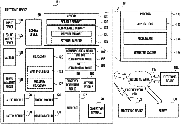
1. An electronic device comprising:
a housing;
an antenna structure disposed in an inner space of the housing and including:
a substrate having a first substrate surface facing toward a first direction, a second substrate surface facing toward a direction opposite to the first substrate surface, and a ground layer disposed in a space between the first substrate surface and the second substrate surface,
at least one conductive patch disposed between the ground layer and the first substrate surface or to be exposed to the first substrate surface, and
at least one power feeder disposed at a position of the at least one conductive patch;
an electronic component disposed on the first substrate surface and disposed to overlap at least in part with the at least one conductive patch when the first substrate surface is viewed from above, the electronic component being electrically connected to a main board through at least one electrical connection structure; and
a wireless communication circuit disposed in the inner space, electrically connected to the at least one power feeder, and configured to form a beam pattern in the first direction through the at least one conductive patch,
wherein the at least one electrical connection structure including:
a first conductive via disposed to pass through the at least one conductive patch and the ground layer, and
a second conductive via passing through the at least one conductive patch and electrically connected to the ground layer.
|