| CPC H01Q 21/065 (2013.01) [G06F 3/0412 (2013.01); H01Q 1/243 (2013.01); H01Q 3/36 (2013.01); H01Q 5/30 (2015.01)] | 17 Claims |
|
1. An electronic device, comprising:
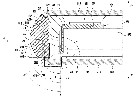
a housing comprising a first plate, a second plate and a side member surrounding a space between the first plate and the second plate, the side member including a conductive portion;
a display positioned within the space to be viewable through at least a part of the first plate, wherein an edge of the display includes a gap from the conductive portion of the side member, wherein the gap is covered by a peripheral portion of the first plate when the first plate is viewed from above and wherein the display includes a display panel and a conductive plate attached to a rear surface of the display panel;
an antenna structure comprising;
a substrate disposed in the space of the housing and extending toward the gap between the display and the conductive portion; and
a plurality of conductive patterns disposed at the substrate, and
at least one wireless communication circuitry configured to transmit or receive a signal through the plurality of conductive patterns and to form a first directivity beam through the peripheral portion of the first plate corresponding to the gap between the display and the conductive portion,
wherein the display includes a cutting part from which at least part of an area overlapping the plurality of conductive patterns is omitted when the first plate is viewed from above,
wherein the cutting part is formed so that the conductive plate and the display panel are cut,
wherein the at least one wireless communication circuitry is configured to form the first directivity beam in a direction toward which the first plate is directed through the cutting part of the conductive plate.
|