| CPC H01L 33/644 (2013.01) [G02B 27/017 (2013.01); H01L 25/0753 (2013.01); H01L 33/62 (2013.01); H01L 33/641 (2013.01); H01L 33/642 (2013.01)] | 20 Claims |
|
1. A device comprising:
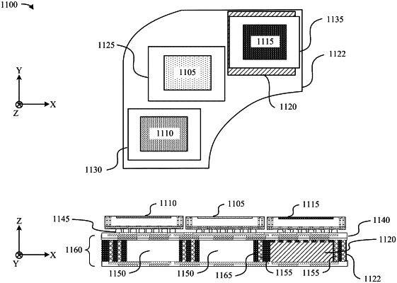
a display package comprising a molding compound, a backplane die, and at least one spacer structure, wherein the backplane die and the at least one spacer structure are embedded within the molding compound; and
a plurality of light emitting diode (LED) dies arranged on a top surface of the display package, the plurality of LED dies including a first die containing an array of red LEDs, a second die containing an array of green LEDs, and a third die containing an array of blue LEDs, wherein:
the first die, the second die, and the third die are individually mounted and spaced apart on the top surface of the display package,
the backplane die includes driver circuits configured to drive LEDs of the first die, the second die, and the third die, and
the at least one spacer structure has a higher thermal conductivity than the molding compound and is configured to dissipate heat generated by the LEDs of the first die, the second die, and the third die.
|