| CPC H01L 33/62 (2013.01) [G09G 3/32 (2013.01); H01L 27/156 (2013.01); H01L 33/005 (2013.01); H01L 33/42 (2013.01); H01L 33/58 (2013.01); G09G 2320/0686 (2013.01); H01L 2933/0066 (2013.01)] | 20 Claims |
|
1. A light-emitting device comprising:
a continuous diode structure that extends over a continuous area of the device and includes first and second doped semiconductor layers and a junction or active layer therebetween that are arranged for emitting light;
a first set of multiple composite electrical contacts, the locations of which define an array of independently operable light-emitters in the continuous diode structure, each composite electrical contact extending over a corresponding discrete areal region of the first semiconductor layer within the continuous area of the device and comprising
an electrically conductive layer,
a transparent dielectric layer between the conductive layer and the first semiconductor layer, and
one or more electrically conductive vias that electrically couple the conductive layer to the first semiconductor layer through the dielectric layer;
a second set of one or more electrical contacts in electrical contact with the second semiconductor layer; and
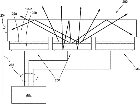
a set of multiple nanostructured optical elements arranged, on or in the first semiconductor layer or on or in the second semiconductor layer, so as to redirect at least a portion of light emitted by the continuous diode structure that propagates laterally in one or more optical modes supported by the continuous diode structure to exit the device through the second semiconductor layer.
|