| CPC H01L 33/62 (2013.01) [H01L 33/486 (2013.01); H01L 33/56 (2013.01)] | 20 Claims |
|
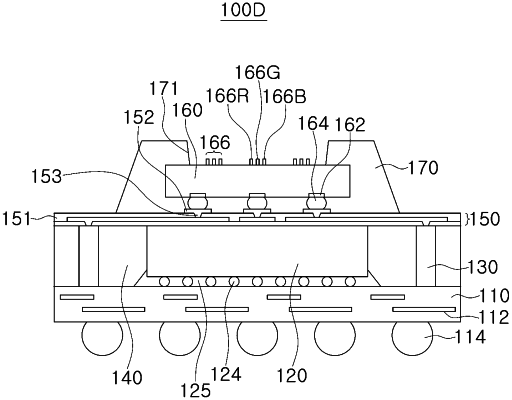
1. A display module package, comprising:
a first wiring member having a first wiring layer;
a semiconductor chip disposed on the first wiring member and electrically connected to the first wiring layer;
a first molding member disposed on the first wiring member and encapsulating at least a portion of the semiconductor chip;
a second wiring member disposed on the semiconductor chip and the first molding member and having a second wiring layer;
a vertical connection electrode disposed between the first wiring member and the second wiring member and electrically connecting the first wiring layer to the second wiring layer;
a light emitting device array disposed on the second wiring member, and including a plurality of connection pads disposed on a first surface facing the second wiring member and a plurality of light emitting devices disposed on a second surface opposite the first surface;
a plurality of conductive bumps disposed between the second wiring member and the light emitting device array, and electrically connecting the plurality of connection pads to the second wiring layer; and
external connection terminals disposed below the first wiring member and electrically connected to the first wiring layer,
wherein the plurality of light emitting devices are electrically connected to the external connection terminals through the plurality of connection pads.
|