| CPC H01L 33/62 (2013.01) [G02B 6/12 (2013.01); H01L 23/488 (2013.01); H01L 31/0224 (2013.01); H01L 31/0232 (2013.01); H01L 33/58 (2013.01)] | 9 Claims |
|
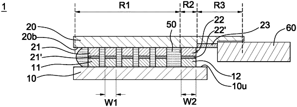
1. An optoelectronic package structure, comprising a photonic component, an electronic component, an optical device disposed on a side of the photonic component, and a filling material,
wherein the photonic component comprises a plurality of bonding pads and at least one blocking pad disposed on the side of the photonic component, the photonic component is electrically connected to the electronic component via the plurality of bonding pads, and the at least one blocking pad is disposed outside the plurality of bonding pads,
wherein the blocking pad is located between the optical device and the plurality of bonding pads, and
wherein the filling material is not disposed between the optical device and the at least one blocking pad and the filling material fills between the plurality of bonding pads.
|