| CPC H01L 33/60 (2013.01) [H01L 25/167 (2013.01); H01L 33/465 (2013.01); H01L 33/502 (2013.01); H01L 33/505 (2013.01); H01L 33/54 (2013.01); H01L 33/62 (2013.01); H01L 24/29 (2013.01); H01L 24/32 (2013.01); H01L 2224/29139 (2013.01); H01L 2224/32145 (2013.01)] | 17 Claims |
|
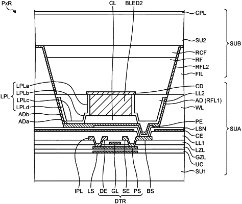
1. A display device comprising:
a first substrate;
a plurality of pixels provided to the first substrate;
a light emitting element provided to each of the pixels;
a phosphor layer covering at least an upper surface of the light emitting element;
a first reflective layer facing a side surface of the light emitting element;
a second reflective layer provided to a side surface of the phosphor layer, separated from the first reflective layer in a normal direction of the first substrate, and disposed farther away from the first substrate than the first reflective layer; and
wherein the first reflective layer is an anode electrode electrically coupled to the light emitting element.
|