| CPC H01L 33/58 (2013.01) [H01L 21/563 (2013.01); H01L 21/6835 (2013.01); H01L 24/00 (2013.01); H01L 33/44 (2013.01); H01L 24/16 (2013.01); H01L 24/32 (2013.01); H01L 24/73 (2013.01); H01L 24/92 (2013.01); H01L 33/62 (2013.01); H01L 2221/68345 (2013.01); H01L 2224/13101 (2013.01); H01L 2224/16225 (2013.01); H01L 2224/73204 (2013.01); H01L 2224/73253 (2013.01); H01L 2224/81005 (2013.01); H01L 2224/81203 (2013.01); H01L 2224/81224 (2013.01); H01L 2224/81815 (2013.01); H01L 2224/92125 (2013.01); H01L 2924/00014 (2013.01); H01L 2924/15311 (2013.01); H01L 2924/18161 (2013.01); H01L 2924/3511 (2013.01)] | 20 Claims |
|
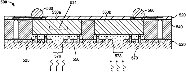
1. A semiconductor device, comprising:
a transmissive layer comprising a transmissive layer first side and a transmissive layer second side opposite the transmissive layer first side, wherein the transmissive layer permits passage of radiation between the transmissive layer first side and the transmissive layer second side;
a first redistribution structure comprising a first redistribution structure first side, a first redistribution structure second side opposite the first redistribution structure first side, and a first redistribution structure opening that extends through the first redistribution structure first side to the first redistribution structure second side and exposes a portion of the transmissive layer first side, wherein the first redistribution structure first side comprises first conductive pads; and
a first component comprising a first component first side, a first component second side opposite the first component first side, and a first radiation circuit, wherein the first component second side is coupled to the first conductive pads of the first redistribution structure first side, and wherein the first radiation circuit is vertically aligned with the first redistribution structure opening to permit radiation to pass between the first radiation circuit and a portion of the transmissive layer via the first redistribution structure opening.
|