| CPC H01L 33/505 (2013.01) [H01L 27/156 (2013.01); H01L 33/0093 (2020.05); H01L 33/08 (2013.01); H01L 33/22 (2013.01); H01L 33/36 (2013.01); H01L 33/382 (2013.01); H01L 33/502 (2013.01); H01L 33/62 (2013.01); F21S 41/153 (2018.01); F21S 41/192 (2018.01); F21Y 2115/10 (2016.08); H01L 2933/0041 (2013.01); H01L 2933/0066 (2013.01)] | 10 Claims |
|
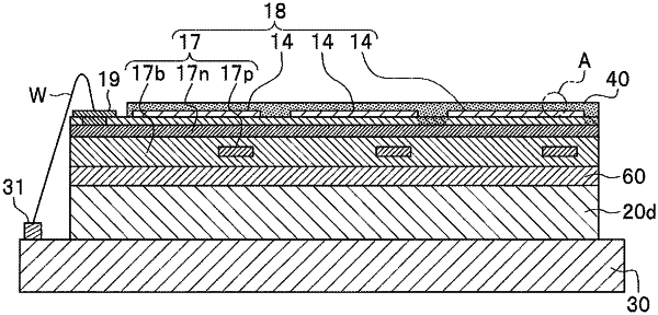
1. A light emitting device comprising:
a base;
a first terminal and a second terminal located at an upper surface of the base;
a light emitting element array chip mounted on the upper surface of the base such that the light emitting element array chip is located between the first terminal and the second terminal, the light emitting element array chip comprising:
a plurality of light emitting elements,
a support substrate having a continuous upper surface that supports the plurality of light emitting elements,
a multilayer wiring structure disposed above the support substrate and comprising a plurality of first wirings, a plurality of second wirings, and an inter-wiring insulating film, wherein the plurality of first wirings are located above the plurality of second wirings with portions of the inter-wiring insulating film located therebetween, wherein each of the light emitting elements is arranged above and electrically connected to one of the first wirings and one of the second wirings;
a plurality of wires including a plurality of first wires connecting the plurality of first wirings to the first terminal, and a plurality of second wires connecting the plurality of second wirings to the second terminal; and
a phosphor layer directly covering the light emitting element array chip so as to collectively cover surfaces of the plurality of light emitting elements, wherein an average layer thickness of the phosphor layer is 50 μm or less.
|