US 11,942,577 B2
Optical device
Ronghui Liu, Beijing (CN); Yuanhong Liu, Beijing (CN); Yanfeng Li, Beijing (CN); Xiaoxia Chen, Beijing (CN); Xiaole Ma, Beijing (CN); and Yuan Xue, Beijing (CN)
Assigned to GRIREM ADVANCED MATERIALS CO., LTD., Beijing (CN)
Appl. No. 17/254,226
Filed by GRIREM ADVANCED MATERIALS CO., LTD, Beijing (CN)
PCT Filed Aug. 22, 2019, PCT No. PCT/CN2019/102048
§ 371(c)(1), (2) Date Dec. 18, 2020,
PCT Pub. No. WO2021/031204, PCT Pub. Date Feb. 25, 2021.
Prior Publication US 2022/0173281 A1, Jun. 2, 2022
This patent is subject to a terminal disclaimer.
Int. Cl. H01L 33/50 (2010.01); C09K 11/77 (2006.01); G02B 5/20 (2006.01); H01L 33/30 (2010.01)
CPC H01L 33/504 (2013.01) [C09K 11/7716 (2013.01); C09K 11/77217 (2021.01); G02B 5/208 (2013.01); H01L 33/30 (2013.01)] 12 Claims
OG exemplary drawing
 
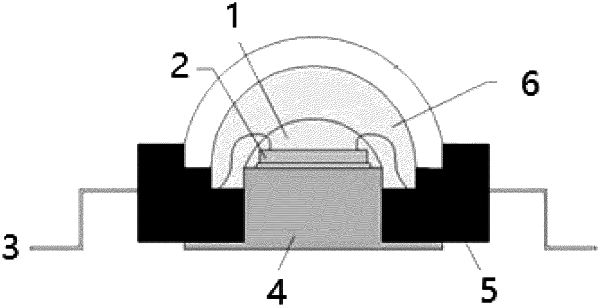
1. An optical device, comprising an LED chip, a light absorber and/or visible-light luminescent material and a near-infrared luminescent material, wherein a luminous power of light emitted by the near-infrared luminescent material and the light absorber and/or visible-light luminescent material in a band of 650-1000 nm under the excitation of the LED chip is A, and a sum of a luminous power of light emitted by the near-infrared and visible-light luminescent materials in a band of 350-650 nm under the excitation of the LED chip and a luminous power of residual light emitted by the LED chip in the band of 350-650 nm after the LED chip excites the near-infrared and visible-light luminescent materials is B, with B/A*100% being 0.1%-10%.