| CPC H01L 33/387 (2013.01) [H01L 33/005 (2013.01); H01L 33/10 (2013.01)] | 13 Claims |
|
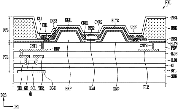
1. A display device comprising:
a first electrode disposed on a substrate;
a first insulating film disposed on the first electrode and having a first opening;
a light-emitting element disposed directly on the first insulating film;
a second insulating film disposed on the first insulating film, contacted with the first insulating film, and having a second opening; and
a contact electrode electrically contacting at least a portion of the first electrode through the first opening and the second opening, wherein
a side surface of the first insulating film defines the first opening, and
the second insulating film overlaps the side surface of the first insulating film such that the contact electrode and the first insulating film are not in contact with each other.
|