| CPC H01L 33/382 (2013.01) [H01L 33/46 (2013.01); H01L 33/62 (2013.01)] | 20 Claims |
|
1. A deep UV light emitting diode, comprising:
a substrate;
an n-type semiconductor layer located on the substrate;
a mesa disposed on the n-type semiconductor layer, and including an active layer and a p-type semiconductor layer;
an n-ohmic contact layer in contact with the n-type semiconductor layer;
a p-ohmic contact layer in contact with the p-type semiconductor layer;
an n-bump electrically connected to the n-ohmic contact layer; and
a p-bump electrically connected to the p-ohmic contact layer, wherein:
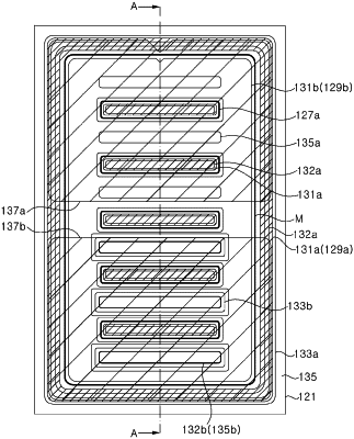
the mesa includes a plurality of vias exposing the n-type semiconductor layer,
the mesa has an elongated rectangular shape along a longitudinal direction,
the vias are arranged parallel to one another in a direction perpendicular to the longitudinal direction, and
the n-ohmic contact layer is formed on the n-type semiconductor layer exposed around the mesa and on the n-type semiconductor layer disposed in the vias, respectively.
|