| CPC H01L 33/20 (2013.01) [F21K 9/90 (2013.01); H01L 24/97 (2013.01); H01L 25/0753 (2013.01); H01L 33/52 (2013.01); H01L 33/64 (2013.01); H01L 33/644 (2013.01); H05K 1/05 (2013.01); H05K 3/0014 (2013.01); H05K 3/284 (2013.01); H10K 19/901 (2023.02); H10K 50/10 (2023.02); F21Y 2115/10 (2016.08); H01L 2924/181 (2013.01); H05K 2201/0129 (2013.01); H05K 2201/10106 (2013.01)] | 18 Claims |
|
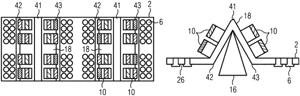
1. A method for producing a semiconductor component comprising one radiation-emitting optical semiconductor chip or a plurality of radiation-emitting optical semiconductor chips, comprising:
applying the radiation-emitting optical semiconductor chip or the plurality of radiation-emitting optical semiconductor chips on a deformable flat carrier, wherein the deformable flat carrier has a plurality of plated through holes,
deforming the carrier and permanently fixing the deformation, wherein the carrier is deformed by bending or curving by way of a shaping part and the bent or curved carrier is casted in order to fix the deformation,
wherein the shaping part is removed after casting and the resultant cavity is filled or the shaping part remains in the deformed carrier after casting, and
wherein the radiation-emitting optical semiconductor chip or the plurality of radiation-emitting optical semiconductor chips is/are arranged in an angular fashion with respect to a base side of the semiconductor component.
|