| CPC H01L 33/10 (2013.01) [H01L 27/156 (2013.01); H01L 33/32 (2013.01); H01L 33/382 (2013.01)] | 31 Claims |
|
1. A light emitting device comprising:
a semiconductor diode structure comprising an active region, a top surface, an oppositely positioned bottom surface, and side surfaces connecting the top and bottom surfaces;
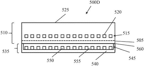
an array of nanoantennas embedded in the semiconductor diode structure between the active region and the top surface; and
a reflector located on the opposite side of the active region from the nanostructured layer,
the array of nanoantennas and the reflector forming an optical cavity that defines a plurality of cavity modes and a density of states, structures and positions of the nanoantennas and the reflector resulting in the cavity modes and density of states being tuned to achieve a selected level of internal quantum efficiency.
|