| CPC H01L 33/0095 (2013.01) [H01L 27/156 (2013.01); H01L 33/62 (2013.01)] | 25 Claims |
|
1. A light-emitting diode (LED) device, comprising:
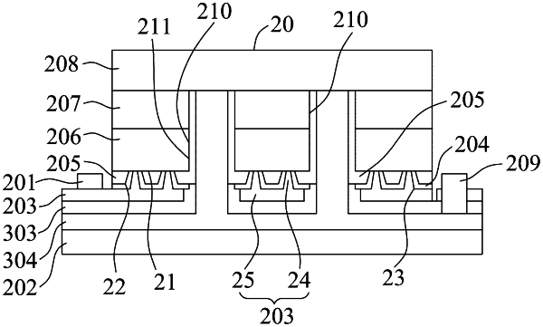
an epitaxial structure including a first-type semiconductor unit having a contact surface, an active layer disposed on said first-type semiconductor unit opposite to said contact surface, and a second-type semiconductor unit disposed on said active layer opposite to said first-type semiconductor unit, said second-type semiconductor unit having a light emitting surface opposite to said first-type semiconductor unit;
a light transmittable dielectric element disposed on said contact surface of said first-type semiconductor unit and formed with at least one first through hole to expose said contact surface;
an adhesive layer disposed on a surface of said light transmittable dielectric element opposite to said first-type semiconductor unit and formed with at least one second through hole disposed in spatial communication with and corresponding positionally to said first through hole, said adhesive layer having a thickness that is at most one fifth of a thickness of said light transmittable dielectric element, and being made of a transparent electrically conductive material; and
a metal contact element disposed on a surface of said adhesive layer opposite to said light transmittable dielectric element, wherein said metal contact element extends into said first and second through holes and electrically contacts said contact surface of said first-type semiconductor unit, wherein said light transmittable dielectric element has at least one hole-defining wall defining said first through hole, wherein said adhesive layer extends into said hole-defining wall, and wherein a width of said second through hole is smaller than a width of said first through hole.
|