US 11,942,566 B2
Thin-film semiconductor optoelectronic device with textured front and/or back surface prepared from etching
Yan Zhu, Dublin, CA (US); Sean Sweetnam, Menlo Park, CA (US); Brendan M. Kayes, Los Gatos, CA (US); Melissa J. Archer, San Jose, CA (US); and Gang He, Cupertino, CA (US)
Assigned to UTICA LEASECO, LLC, Rochester Hills, MI (US)
Filed by Utica Leaseco, LLC, Rochester Hills, MI (US)
Filed on Jun. 14, 2021, as Appl. No. 17/347,314.
Application 17/347,314 is a division of application No. 15/422,218, filed on Feb. 1, 2017, granted, now 11,038,080.
Application 15/422,218 is a continuation in part of application No. 15/340,560, filed on Nov. 1, 2016, granted, now 10,008,628, issued on Jun. 26, 2018.
Application 15/340,560 is a continuation of application No. 14/452,393, filed on Aug. 5, 2014, granted, now 9,502,594, issued on Nov. 22, 2016.
Application 14/452,393 is a continuation in part of application No. 13/354,175, filed on Jan. 19, 2012, granted, now 9,136,422, issued on Sep. 15, 2015.
Prior Publication US 2021/0305452 A1, Sep. 30, 2021
Int. Cl. H01L 33/00 (2010.01); H01L 31/0216 (2014.01); H01L 31/0236 (2006.01); H01L 31/056 (2014.01); H01L 31/18 (2006.01); H01L 33/22 (2010.01); H01L 33/30 (2010.01); H01L 33/42 (2010.01); H01L 33/44 (2010.01); H01L 33/46 (2010.01)
CPC H01L 33/0093 (2020.05) [H01L 31/02168 (2013.01); H01L 31/02366 (2013.01); H01L 31/056 (2014.12); H01L 31/1892 (2013.01); H01L 33/0062 (2013.01); H01L 33/22 (2013.01); H01L 33/30 (2013.01); H01L 33/42 (2013.01); H01L 33/44 (2013.01); H01L 33/46 (2013.01); H01L 2933/0016 (2013.01); H01L 2933/0025 (2013.01); H01L 2933/0091 (2013.01); Y02E 10/52 (2013.01)] 10 Claims
OG exemplary drawing
 
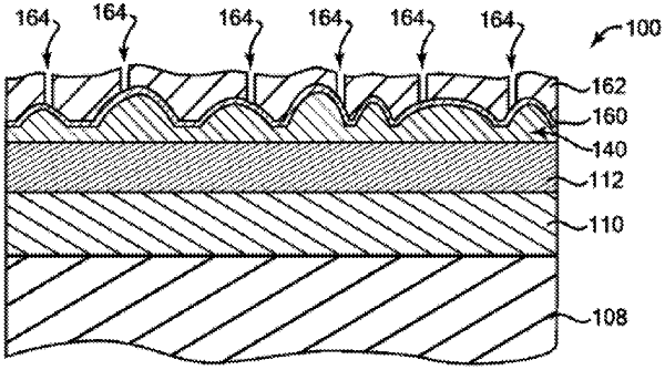
1. A method for providing at least one textured layer in an optoelectronic device, the method comprising:
forming a reflective back metal layer having a flat surface;
forming an absorber layer on the reflective back metal layer to have a first thickness;
epitaxially growing a semiconductor layer to have a second thickness less than the first thickness of the absorber layer, with the semiconductor layer being positioned between the flat surface of the reflective back metal layer and the absorber layer; and
positioning an emitter layer between the absorber layer and the semiconductor layer, wherein the emitter layer and the absorber layer form a p-n junction of the optoelectronic device, wherein the absorber layer is further positioned between the semiconductor layer and a surface of the optoelectronic device on which light is to be incident.