| CPC H01L 31/1864 (2013.01) [H01L 31/0682 (2013.01); H01L 31/1804 (2013.01); Y02E 10/547 (2013.01); Y02P 70/50 (2015.11)] | 18 Claims |
|
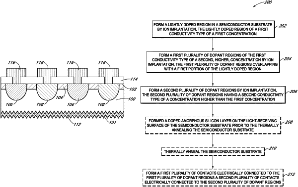
1. A method of fabricating a solar cell, the method comprising:
forming a lightly doped region in a semiconductor substrate by a first ion implantation, the lightly doped region of a first conductivity type of a first concentration;
forming a first plurality of dopant regions of the first conductivity type of a second, higher, concentration by a second ion implantation, the first plurality of dopant regions overlapping with a first portion of the lightly doped region;
forming a second plurality of dopant regions by a third ion implantation, the second plurality of dopant regions having a second conductivity type of a concentration higher than the first concentration, and the second plurality of dopant regions overlapping with a second portion of the lightly doped region and alternating with but not overlapping the first plurality of dopant regions;
thermally annealing the semiconductor substrate subsequent to the third ion implantation;
forming a tunneling dielectric layer on a light-receiving surface of the semiconductor substrate;
forming a doped amorphous silicon layer on the tunneling dielectric layer on the light-receiving surface of the semiconductor substrate prior to the thermally annealing the semiconductor substrate; and
crystallizing the doped amorphous silicon layer during the thermally annealing the semiconductor substrate to form a doped polycrystalline silicon layer on the light-receiving surface of the semiconductor substrate.
|