| CPC H01L 31/03529 (2013.01) [H01L 31/02005 (2013.01)] | 10 Claims |
|
1. A chip package, comprising:
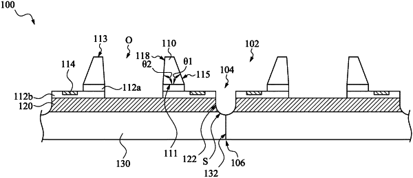
a chip having a conductive pad, an opening defining a sensing area, an inner wall surface surrounding the opening, and an outer wall surface facing away from the inner wall surface;
a carrier; and
a light-transmissive function layer located between the chip and the carrier, wherein a first portion of the light-transmissive function layer is located in the opening, a second portion of the light-transmissive function layer is covered by the chip, a third portion of the light-transmissive function layer protrudes from the outer wall surface of the chip, and the conductive pad is located on the third portion, wherein a first included angle is formed between the outer wall surface of the chip and a surface of the chip facing the light-transmissive function layer, and a second included angle is formed between the inner wall surface and the surface of the chip facing the light-transmissive function layer, and the first included angle is different from the second included angle.
|