| CPC H01L 29/872 (2013.01) [H01L 21/8252 (2013.01); H01L 27/0629 (2013.01); H01L 29/417 (2013.01); H01L 29/66143 (2013.01); H01L 29/868 (2013.01); H01L 29/2003 (2013.01); H01L 29/205 (2013.01)] | 17 Claims |
|
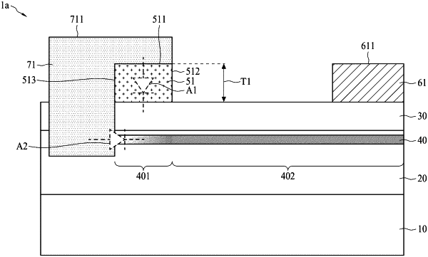
1. A semiconductor device structure, comprising:
a substrate;
a first nitride semiconductor layer disposed on the substrate;
a second nitride semiconductor layer disposed on the first nitride semiconductor layer and having a bandgap greater than that of the first nitride semiconductor layer;
a third nitride semiconductor layer disposed on the second nitride semiconductor layer;
a first electrode disposed on the second nitride semiconductor layer and horizontally spaced apart from the third nitride semiconductor layer; and
a second electrode covering an upper surface of the third nitride semiconductor layer and in direct contact with the first nitride semiconductor layer,
wherein the second electrode has a reversed L shape, and comprises a first part covering the third nitride semiconductor layer, and a second part penetrating the second nitride semiconductor layer and extending into the first nitride semiconductor layer, wherein a depth of the extending is less than a thickness of the first nitride semiconductor layer.
|