US 11,942,559 B2
Method of preventing TFT from ESD damaging, method of manufacturing TFT, and display panel
Junzheng Liu, Guangdong (CN)
Assigned to Shenzhen China Star Optoelectronics Semiconductor Display Technology Co., Ltd., Shenzhen (CN)
Appl. No. 17/600,281
Filed by Shenzhen China Star Optoelectronics Semiconductor Display Technology Co., Ltd., Guangdong (CN)
PCT Filed Aug. 19, 2021, PCT No. PCT/CN2021/113482
§ 371(c)(1), (2) Date Sep. 30, 2021,
PCT Pub. No. WO2023/015591, PCT Pub. Date Feb. 16, 2023.
Claims priority of application No. 202110912249.X (CN), filed on Aug. 10, 2021.
Prior Publication US 2024/0021732 A1, Jan. 18, 2024
Int. Cl. G06T 7/00 (2017.01); H01L 27/02 (2006.01); H01L 27/12 (2006.01); H01L 29/24 (2006.01); H01L 29/786 (2006.01)
CPC H01L 29/78696 (2013.01) [H01L 27/027 (2013.01); H01L 27/1233 (2013.01)] 17 Claims
OG exemplary drawing
 
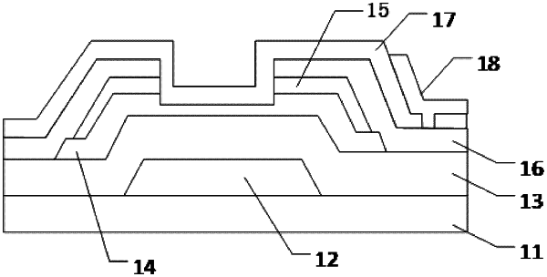
1. A method of preventing thin-film transistor (TFT) from electrostatic discharge (ESD) damaging, comprising following steps:
acquiring a test data of at least one film layer of a plurality of TFTs, the test data comprising manufacturing parameters of each film layer and electrostatic discharge voltages that each film layer can withstand;
data fitting the test data to obtain at least one fitting curve; and
acquiring a relationship between an anti-ESD capability of the TFT and the manufacturing parameters of each film layer from the fitting curve.