| CPC H01L 29/78696 (2013.01) [H01L 29/0665 (2013.01); H01L 29/41775 (2013.01); H01L 29/42392 (2013.01); H01L 29/66545 (2013.01)] | 12 Claims |
|
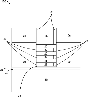
1. A semiconductor nanosheet device comprising:
semiconductor channel layers vertically aligned and stacked one on top of another, the semiconductor channel layers separated by a work function metal; and
a second layer sandwiched between two first layers, the second layer and the two first layers are below the semiconductor channel layers and above a substrate, wherein vertical side surfaces of the semiconductor channel layers are vertically aligned with vertical side surfaces of an upper layer of the two first layers, wherein a combined thickness of the second layer and the two first layers is approximately the same as a thickness of the work function metal between the semiconductor channel layers.
|