| CPC H01L 29/7869 (2013.01) [H01L 29/42384 (2013.01); H01L 29/66969 (2013.01); H01L 29/78606 (2013.01); H01L 29/78618 (2013.01); H01L 29/78648 (2013.01); H01L 29/78696 (2013.01)] | 18 Claims |
|
1. A semiconductor device comprising a pixel portion,
wherein the pixel portion comprises a transistor and a light emitting element electrically connected to the transistor,
wherein the transistor comprises:
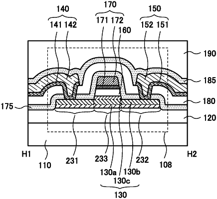
an oxide semiconductor layer comprising In, Ga, and Zn;
a gate insulating layer over the oxide semiconductor layer;
a gate electrode overlapping with the oxide semiconductor layer with the gate insulating layer provided therebetween, the gate electrode comprising a first layer and a second layer provided over the first layer;
a first insulating layer over the gate electrode, the first insulating layer having a region being in contact with a top surface of the gate insulating layer; and
a first conductive layer over the first insulating layer, a part of the first conductive layer connected to the oxide semiconductor layer through an opening provides the first insulating layer,
wherein in a cross-sectional view parallel to a channel length direction of the transistor, an end portion of the first layer of the gate electrode is positioned on an outer side than an end portion of the second layer of the gate electrode,
wherein in the cross-sectional view parallel to the channel length direction of the transistor, the oxide semiconductor layer comprises:
a channel formation region;
a first region being adjacent to the channel formation region and being in contact with the gate insulating layer;
a second region being adjacent to the first region and being in contact with the first insulating layer; and
a third region being in contact with the part of the first conductive layer, and wherein the first region is thicker than the second region and the third region.
|