| CPC H01L 29/7869 (2013.01) [H01L 29/04 (2013.01); H01L 29/423 (2013.01); H01L 29/42384 (2013.01); H01L 29/49 (2013.01); H01L 29/4908 (2013.01); H01L 29/66969 (2013.01); H01L 29/78633 (2013.01); H01L 29/78648 (2013.01); G02F 1/1368 (2013.01); H01L 21/426 (2013.01); H01L 27/1225 (2013.01); H10K 50/115 (2023.02); H10K 59/12 (2023.02); H10K 59/40 (2023.02)] | 3 Claims |
|
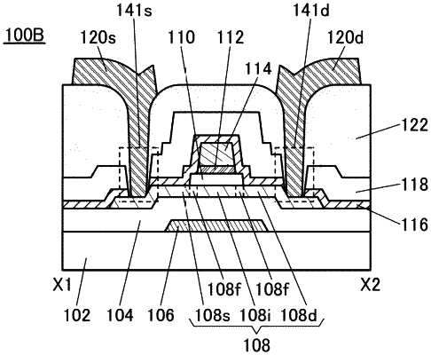
1. A semiconductor device comprising:
a first conductive film;
a first insulating film over the first conductive film;
a first semiconductor film, having a region overlapping with the first conductive film, over the first insulating film;
a second insulating film having a region in contact with a top surface of the first semiconductor film;
a second conductive film, having a region overlapping with the first semiconductor film, over the second insulating film;
a third insulating film comprising silicon nitride and having a region in contact with a top surface of the second conductive film, a region in contact with a side surface of the second conductive film, and a region in contact with a top surface of the second insulating film;
a fourth insulating film comprising silicon oxide and having a region in contact with a top surface of the third insulating film;
a fifth insulating film comprising an organic material and having a region in contact with a top surface of the fourth insulating film;
a third conductive film and a fourth conductive film over the fifth insulating film;
a pixel electrode of a liquid crystal element electrically connected to the fourth conductive film; and
a common electrode overlapping with the pixel electrode and the third conductive film,
wherein the first semiconductor film comprises a channel formation region of a transistor,
wherein the second conductive film is configured to function as a gate electrode of the transistor,
wherein the third conductive film is configured to function as one of a source electrode and a drain electrode of the transistor,
wherein the fourth conductive film is configured to function as the other of the source electrode and the drain electrode of the transistor,
wherein the third insulating film and the fourth insulating film comprise a first opening and a third opening,
wherein the fifth insulating film comprises a second opening overlapping with the first opening,
wherein in a cross-sectional view, an upper edge of the first opening is not aligned with a lower edge of the second opening,
wherein a diameter of the second opening at the lower edge of the second opening is larger than a diameter of the first opening at the upper edge of the first opening,
wherein the third conductive film has a region in contact with a top surface of the fifth insulating film and a region in contact with the top surface of the first semiconductor film in a region where the first opening and the second opening overlap with each other,
wherein a spacer overlaps with the first semiconductor film with the third conductive film provided therebetween,
wherein the first semiconductor film is in contact with the fourth conductive film in the third opening, and
wherein the pixel electrode overlaps with the third opening.
|