| CPC H01L 29/7869 (2013.01) [H01L 29/66757 (2013.01); H10B 41/20 (2023.02); H10B 41/23 (2023.02); H10B 41/27 (2023.02); H10B 41/60 (2023.02); H10B 41/70 (2023.02); H10B 43/23 (2023.02); H10B 43/27 (2023.02); H10B 51/20 (2023.02); H10B 53/20 (2023.02); H10B 63/84 (2023.02); H10B 63/845 (2023.02)] | 14 Claims |
|
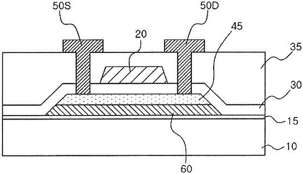
1. A method for fabricating a semiconductor device, the method comprising:
sequentially forming a liner film and a metal oxide film on a substrate, the liner film including a transition metal and being in contact with the metal oxide film;
crystallizing the metal oxide film through an annealing process;
forming a liner pattern and a metal oxide pattern on the substrate by patterning the liner film and the metal oxide film;
forming an insulating film extending along a sidewall of the liner pattern, a sidewall of the metal oxide pattern, and an upper surface of the metal oxide pattern; and
forming a gate electrode on the insulating film,
wherein the annealing process is performed in a nitrogen atmosphere or an oxygen atmosphere.
|