| CPC H01L 29/78618 (2013.01) [H01L 21/02532 (2013.01); H01L 21/02603 (2013.01); H01L 21/823807 (2013.01); H01L 21/823814 (2013.01); H01L 21/823828 (2013.01); H01L 21/823864 (2013.01); H01L 21/823878 (2013.01); H01L 27/092 (2013.01); H01L 29/0653 (2013.01); H01L 29/0673 (2013.01); H01L 29/42392 (2013.01); H01L 29/66545 (2013.01); H01L 29/66553 (2013.01); H01L 29/66742 (2013.01); H01L 29/78696 (2013.01)] | 20 Claims |
|
1. A semiconductor device comprising:
a first gate-all-around field effect transistor (GAA FET) and a second GAA FET; and
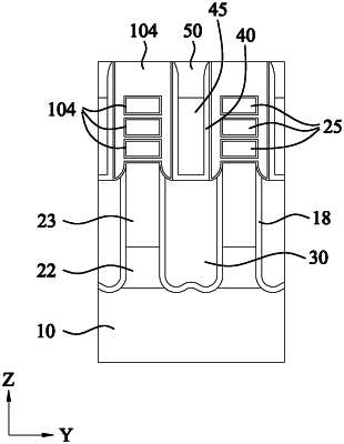
a wall fin disposed between the first GAA FET and the second GAA FET and disposed on an isolation insulating layer, wherein:
the first and second GAA FETs include semiconductor wires or sheets, a gate dielectric layer wrapping around channel regions of the semiconductor wires or sheets, a gate electrode on the gate dielectric layer and a source/drain epitaxial layer,
the wall fin includes a first dielectric layer, a second dielectric layer disposed over the first dielectric layer and a third dielectric layer,
the first, second and third dielectric layers are made of different materials from each other,
the third dielectric layer includes a dielectric material having a dielectric constant higher than the first and second dielectric layers and the isolation insulating layer, and
a fourth dielectric layer different from the first, second and third dielectric layers is disposed on the source/drain epitaxial layer.
|