| CPC H01L 29/78618 (2013.01) [H01L 21/02532 (2013.01); H01L 21/02603 (2013.01); H01L 29/0673 (2013.01); H01L 29/165 (2013.01); H01L 29/42392 (2013.01); H01L 29/66545 (2013.01); H01L 29/66553 (2013.01); H01L 29/66636 (2013.01); H01L 29/66742 (2013.01); H01L 29/7848 (2013.01); H01L 29/78696 (2013.01)] | 20 Claims |
|
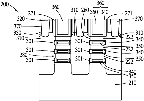
1. A nanosheet semiconductor device, comprising:
a channel region including at least one nanosheet;
a first source/drain region and a second source/drain region separated from each other by the channel region in a horizontal direction;
a gate structure including an upper gate portion disposed over the channel region and a lower gate portion surrounding the at least one nanosheet;
a dummy spacer laterally covering the upper gate portion of the gate structure and having a first surface in contact with the upper gate portion of the gate structure and a second surface opposite to the first surface;
a contact etch stop layer disposed to cover a corresponding one of the first source/drain region and the second source/drain region, the contact etch stop layer including a bottom portion that includes a flat main part and an inclined edge part inclined outwardly and downwardly from the flat main part in the horizontal direction; and
an inner spacer laterally covering the lower gate portion of the gate structure,
the at least one nanosheet including a lateral surface contacting a corresponding one of the first and second source/drain regions, the inner spacer including a lateral surface contacting the corresponding one of the first and second source/drain regions, and the lateral surface of the at least one nanosheet being indented relative to the lateral surface of the inner spacer,
the inclined edge part of the bottom portion of the contact etch stop layer extending to terminate at a position of the second surface of the dummy spacer to divide the second surface of the dummy spacer into a lower surface portion and an upper surface portion, the lower surface portion of the second surface of the dummy spacer extending in a vertical direction perpendicular to the horizontal direction.
|