| CPC H01L 29/785 (2013.01) [H01L 21/0214 (2013.01); H01L 21/02211 (2013.01); H01L 21/02263 (2013.01); H01L 21/76224 (2013.01); H01L 21/76232 (2013.01); H01L 21/823481 (2013.01); H01L 27/0924 (2013.01); H01L 29/517 (2013.01); H01L 29/66545 (2013.01); H01L 29/66795 (2013.01); H01L 29/66818 (2013.01); H01L 21/76227 (2013.01)] | 20 Claims |
|
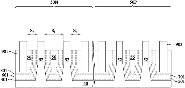
1. A method of manufacturing a semiconductor device, the method comprising:
lining a semiconductor fin with a first liner;
lining the semiconductor fin with a second liner different from the first liner;
lining the semiconductor fin with a third liner different from the second liner;
annealing the third liner to form silicon oxide;
lining the semiconductor fin with a fourth liner different from the third liner;
depositing a capping layer over the fourth liner;
annealing the capping layer to transform the capping layer to silicon oxide;
depositing a dielectric cap over the capping layer;
planarizing the dielectric cap to the semiconductor fin; and
exposing a sidewall of the semiconductor fin.
|